Semiconductor
To provide an efficient and stable one-stop semiconductor equipment supplier
The SEMI BU focuses on testing equipment related to semiconductor industry chain and makes future strategic layout for other advanced semiconductor process equipment. The products include wafer inspection, SiP packaging test, SoC chip test, CIS chip test, BMS chip test, RF chip test , AOI defect inspection and other services.
-
ATE
-
Handler
-
AOI
-
BMS Testing Equipment
-
Consumables

Features and Advantages
The SEMI BU is in charge of the core technologies of chip electrical measurement, optical measurement, image measurement, high-precision automatic control technology and reliability contact mating technology. With the advantages of multi-disciplinary comprehensive capabilities domestic and overseas, the SEMI BU provides the customers with high-efficiency and low-cost one-stop testing solutions. At the same time, it also has achieved breakthroughs in core technologies on many advanced testing equipment. The products have been recognized by customers, and have successfully obtained mass production orders in the semiconductor industry globally.
-

 Technology
Independent R&D, efficient, stable and fully functional software testing platform
-

 Products
Turnkey solutions for testing machines, sorting machines, AOI and consumables
-

 Delivery Time
Standardized products, short delivery time
-

 Technical Team
Nearly 100 AE and FSE engineers
-
-
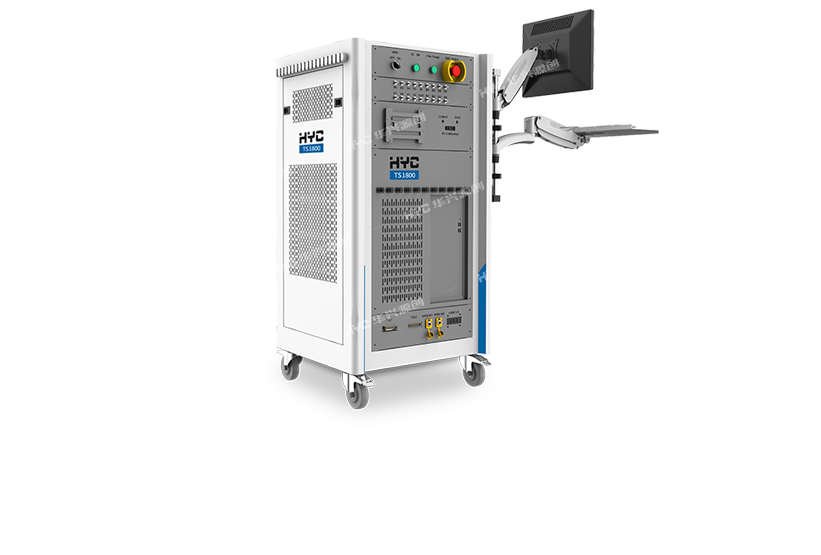
T7600 series SoC Digital ATE
- 6 slots(T7600S)Digital channels support up to 768channelsPower channels support 72channels
- 12 slots(T7600M)Digital channels support up to 1536channelsPower channels support 144channels
- 18 slots(T7600H)Digital channels support up to 2304channelsPower channels support 216channels
- Digital board DP128128 digital channels, 400Mbps, DPS 12channels, RVS 4channels, BPMU 4channels
- FVI32 floating voltage boardSupport up to 32 channelsVoltage range: ±10VVoltage accuracy: ≤±0.5mVMAX current: 38.4A(1.2A/channel)Support Gang
- DPS64 power boardSupport up to 64 channelsVoltage Range: -2.5~8VCurrent output 1.5A/channelGanged up to 96A
- MX32 analog boardHS: 0~250MHz, HR: 0~40KHz,
THD -115dBVarious channel configuration methods16 HS AWG+16 HS DIG16 HR AWG+16 HR DIG8 HS AWG + 8 HS DIG + 8 HR AWG+8 HR DIG
-
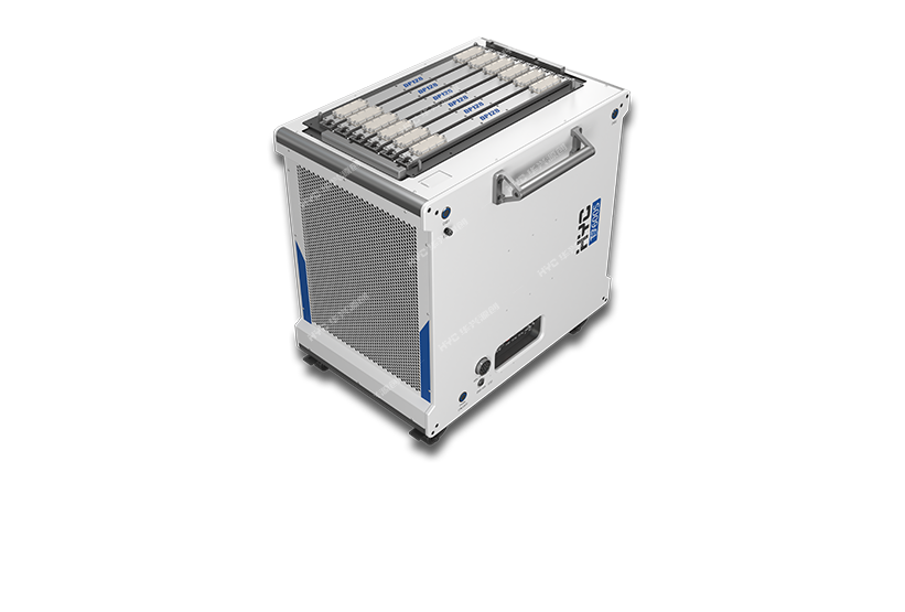
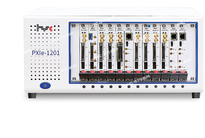
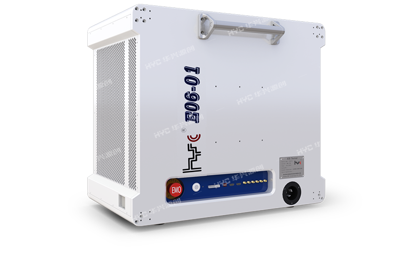
PXIe Platform Testing Equipment
- Two chassis6-slot PXIe-C0601, 12-slot PXIe-C1201
- A variety of self-developed boardsdigital boards, power boards, analog boards and RF boards, etc
- Compatible with other brand systems
- With self-developed multi-function software development platform
-
CIS ATE
- Support up to 16 Sites Parallel Testing
- Support MIPI, DVP and LVDS interfaceMIPI supports up to 1.6Gbps/laneLVDS supports up to 1.0Gbps/lane
- DC Performance192 DC channels and 96 power channels
- Digital PerformanceDigital supports up to 384 channels, 400Mbps
-
RF CHIP TESTER
- Test frequency up to 6GHz, power up to 35dBm
- Support SPI, MIPI and custom digital communication libraries
- Noise Figure measurement: Support Y-Factor and Cold Noise methods
- 32 bidirectional RF ports with 8 input and 8 output for high power
- Domestic chip leading enterprises stable mass production
-
-
-
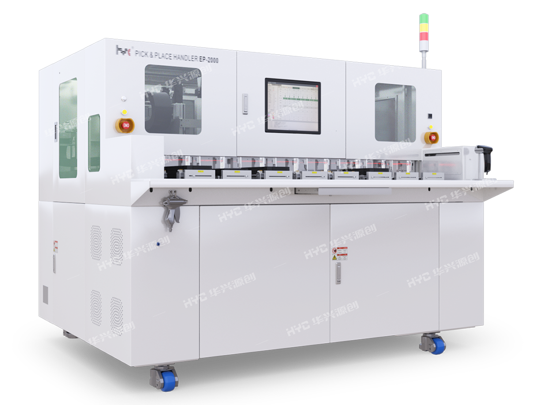
16 Site CIS PnP Handler
- Support up to 16 Sites Parallel Testing
- Support self-contained light source or other types of light source
- MAX UPH:4,500
- MIN size of product can be tested
2mm×2mm
-
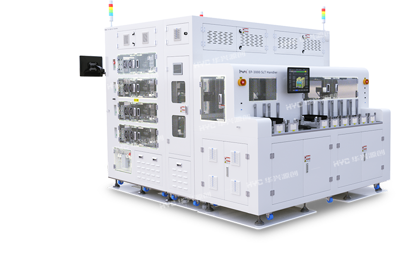
128 Site PnP Handler
- Support up to 128 Sites Parallel Testing
- UPH>11,000 (T.T.>30s)
- Jam Rate<1/5000
- MIN size of product can be tested2mm×2mm
- Support QR code, character and chip recognition
- Support SECS/GEM with completed analysis Tool
- Handler + PXIe all-in-one platform solution
-
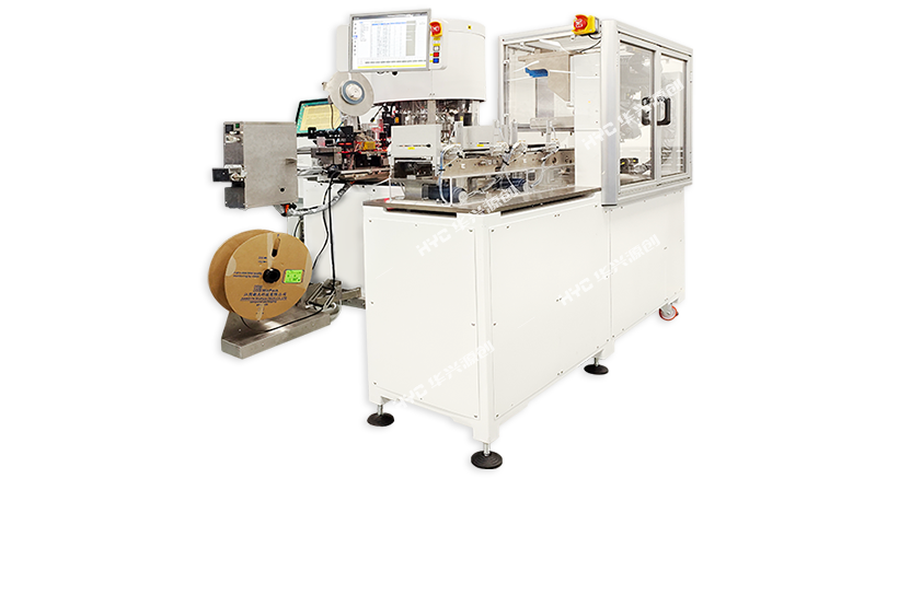
Turret Handler
- Two models20stations、32stations
- Support six-surface inspection
- Support QFN, DFN, SOIC and other packages
- UPH>30,000
- MTBA>1h
-
-
-
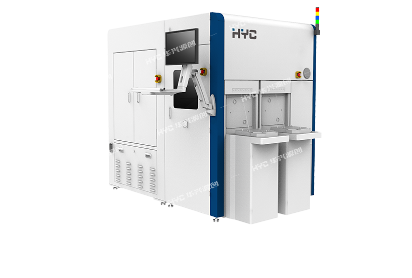
Wafer Macroscopic Defect AOI Solution
- Deploying precise mobile platform in positioning with super-high HFR(high frame rate) data acquisition capability, to improve the customer’s productivity
- Possessing sub-micron optical resolution, able to detect the defects in manufacturing
- Supporting BF/DF multi-mode imaging, thus to display the defects more intuitively
- Employing deep learning algorithms for an automatic defect classification, to realize manpower and cost saving
-
-
-
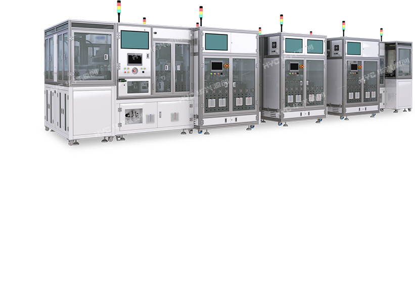
BMS Automatic Testing Solution
- Independently developed battery management chip testing equipment
- Completely replace manual operation
- Data is uploaded to the client MES system in real time
- Designated products of international leading mobile phone enterprises
- Automatic loading and unloading of carriers and life management
- Available for most of the BMS chip testing, BMU and battery pack testing
- High precision detection in ultra wide voltage and current range
- Minimum measuring accuracy: voltage 0.3mV, current 0.4μA
- Follow general instrument testing standards both domestic and overseas
-
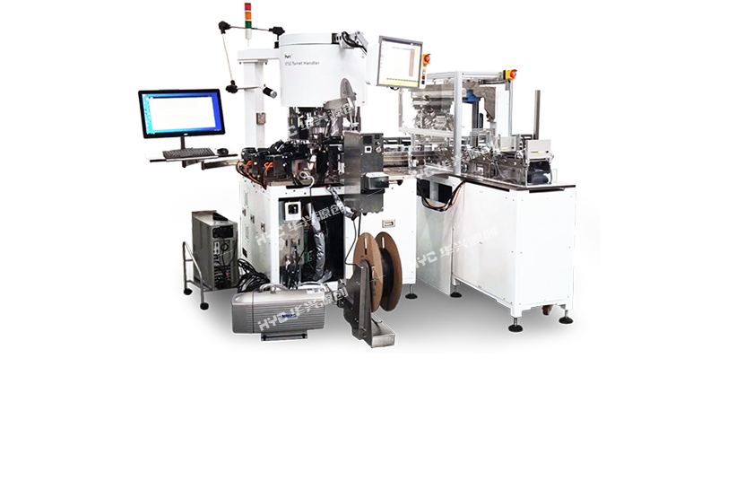
Six-surface Automatic Testing Equipment
- UPH up to 15k, six-surface visual inspection
- Tray in mode effectively avoids secondary damage of high-end chips
- AI algorithms are combined with traditional algorithms to customize the optical system
- OCR/Code reading includes defect types on all sides
-


.png2.png)